Multiferroic BiFeO₃ Thin Film for Spintronics Market to Reach USD 498.3M by 2034 | 10.5% CAGR
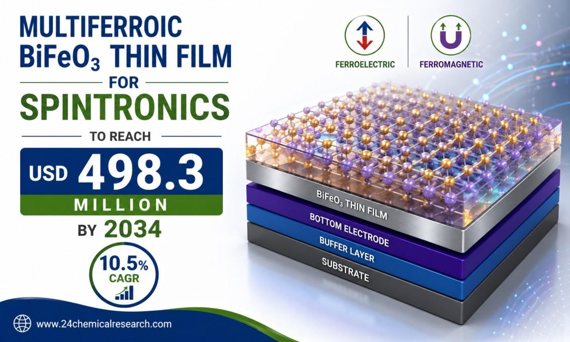
Global Multiferroic (BiFeO₃) Thin Film for Spintronics Device Market size was valued at USD 187.4 million in 2025. The market is projected to grow from USD 204.6 million in 2026 to USD 498.3 million by 2034, exhibiting a remarkable CAGR of 10.5% during the forecast period.
Multiferroic bismuth ferrite (BiFeO₃) thin films are advanced functional materials that simultaneously exhibit ferroelectric and antiferromagnetic ordering, making them uniquely suited for next-generation spintronics device applications. These thin films enable the electrical control of magnetic states — a critical capability in the development of low-power, high-speed memory and logic devices. Key application areas include magnetoelectric random-access memory (MeRAM), spin-orbit torque devices, tunnel junctions, and non-volatile logic elements, where the coupling between ferroelectric polarization and spin transport properties is fundamentally exploited. Unlike conventional semiconductor materials, BiFeO₃ stands apart because it is one of the very few single-phase multiferroic compounds that exhibits both ferroelectric and antiferromagnetic order well above room temperature — a combination that makes it practically viable for real-world device integration without the need for cryogenic conditions.
Get Full Report Here: https://www.24chemicalresearch.com/reports/308879/multiferroic-thin-film-for-spintronics-device-market
Market Dynamics:
The market's trajectory is shaped by a complex interplay of powerful growth drivers, significant restraints that are being actively addressed, and vast, untapped opportunities.
Powerful Market Drivers Propelling Expansion
-
Surging Demand for Low-Power, High-Speed Memory and Logic Devices: The global push toward energy-efficient computing has placed multiferroic BiFeO₃ thin films squarely at the center of next-generation spintronics research and commercialization efforts. Unlike conventional semiconductor devices that rely on charge-based switching, spintronics devices exploit the intrinsic spin of electrons, drastically reducing power dissipation during operation. BiFeO₃ thin films, which simultaneously exhibit ferroelectric and antiferromagnetic ordering at room temperature, offer a rare platform for electrically controlled spin manipulation — a property that is both scientifically significant and commercially compelling. As data center energy consumption continues to rise globally, device architects and materials scientists are converging on multiferroic-based heterostructures as a credible route toward sub-femtojoule switching logic, making this one of the most consequential demand vectors shaping market growth over the forecast horizon.
-
Progress in Thin Film Deposition Technologies Enabling Commercial Scalability: Advances in thin film deposition techniques — including pulsed laser deposition (PLD), molecular beam epitaxy (MBE), and chemical vapor deposition (CVD) — have substantially improved the crystalline quality, stoichiometric control, and reproducibility of BiFeO₃ thin films on technologically relevant substrates such as silicon, SrTiO₃, and DyScO₃. These improvements have directly addressed one of the longstanding barriers to device-grade BiFeO₃ integration: the tendency toward secondary phase formation and bismuth volatility during high-temperature processing. Enhanced epitaxial control now allows researchers and early-stage manufacturers to tailor the ferroelectric polarization axis and the spin cycloid wavelength of BiFeO₃ with precision, enabling device-specific optimization of magnetoelectric coupling coefficients. Furthermore, the compatibility of BiFeO₃ thin film processing with existing CMOS-adjacent fabrication infrastructure has encouraged semiconductor foundries and research consortia in East Asia, North America, and Europe to increase capital allocation toward multiferroic spintronics pilot lines, reinforcing the demand-side fundamentals of this market.
-
Government and Defense Sector Investment in Spintronic and Neuromorphic Computing: National funding bodies and defense agencies across the United States, European Union, Japan, South Korea, and China have identified spintronics and magnetoelectric multiferroics as strategic priority areas within their broader quantum and advanced materials research programs. Programs under agencies such as DARPA, the European Research Council, and Japan's JST have specifically funded projects exploring BiFeO₃-based tunnel junctions, voltage-controlled magnetic anisotropy (VCMA) devices, and magnetoelectric random-access memory (MeRAM) architectures. This sustained governmental support accelerates the transition of BiFeO₃ thin film technology from academic laboratories toward prototype device validation, providing a consistent and long-duration driver for market growth that is relatively insulated from short-term commercial cycle fluctuations. Leading organizations including IBM Research, imec, and several national laboratories are actively advancing BiFeO₃-based device integration, reinforcing the long-term commercial viability of this market.
Download FREE Sample Report: https://www.24chemicalresearch.com/download-sample/308879/multiferroic-thin-film-for-spintronics-device-market
Significant Market Restraints Challenging Adoption
Despite its considerable promise, the market faces meaningful structural and technical hurdles that must be addressed before BiFeO₃ thin films can transition from specialized research applications to mainstream spintronic device manufacturing at scale.
-
High Cost and Limited Throughput of Epitaxial Thin Film Fabrication: The production of device-grade BiFeO₃ thin films with the crystalline perfection required for spintronics applications relies heavily on PLD and MBE — techniques characterized by low deposition rates, small substrate coverage areas, and capital-intensive equipment costs. While these methods deliver the stoichiometric precision and epitaxial quality necessary for research and prototype devices, their throughput limitations and high cost-per-wafer present a formidable restraint on scaling BiFeO₃ thin film manufacturing beyond niche, low-volume applications. Transitioning to higher-throughput deposition methods such as sputtering or metal-organic chemical vapor deposition (MOCVD) without sacrificing the crystalline and functional properties essential for spintronics performance remains an unresolved process engineering challenge, effectively restraining the market's ability to serve cost-sensitive, high-volume device segments.
-
Competition from Established and Emerging Non-Multiferroic Spintronics Platforms: The broader spintronics device market encompasses a range of competing material platforms — including giant magnetoresistance (GMR) multilayers, spin-transfer torque magnetic RAM (STT-MRAM) based on MgO tunnel barriers, and voltage-controlled magnetic anisotropy devices using heavy metal/ferromagnet interfaces — many of which have achieved significantly greater manufacturing maturity and demonstrated device reliability than BiFeO₃-based alternatives. STT-MRAM in particular has crossed into commercial production at leading semiconductor manufacturers, establishing a performance and cost benchmark that multiferroic spintronics devices must credibly surpass or differentiate against to capture meaningful market share. This competitive landscape restrains near-term adoption of BiFeO₃ thin film devices, as system integrators and fabless design firms face limited incentive to redesign around an immature material platform when proven spintronic solutions are already available through established supply chains.
Critical Market Challenges Requiring Innovation
The transition from laboratory success to device-level reliability in spintronic applications presents its own distinct set of challenges for BiFeO₃ thin films. Persistent leakage current issues — originating from oxygen vacancies, Fe²⁺/Fe³⁺ mixed valence states, and grain boundary conduction pathways — continue to undermine polarization switching reliability and degrade retention characteristics in memory applications. For spintronics device applications where precise, reproducible switching is a functional prerequisite, uncontrolled leakage remains a technically limiting obstacle that the materials community has not yet resolved at industrially relevant film thicknesses and deposition throughputs.
Additionally, the market contends with a lack of standardized characterization and benchmarking protocols. The multiferroic spintronics field currently lacks universally adopted standards for measuring and reporting key device figures of merit — including magnetoelectric coupling coefficients, tunnel magnetoresistance ratios in BiFeO₃-based magnetic tunnel junctions, and endurance cycling performance. This absence of standardization makes cross-laboratory comparisons difficult, slows the pace of iterative device optimization, and creates barriers for investors and procurement decision-makers attempting to evaluate the commercial maturity of competing BiFeO₃ device architectures. Until industry consortia or standards bodies establish agreed-upon benchmarking frameworks, the market will continue to face challenges in demonstrating unambiguous performance advantages over incumbent memory technologies.
Vast Market Opportunities on the Horizon
-
BiFeO₃-Based Magnetoelectric RAM as a Next-Generation Non-Volatile Memory Architecture: Magnetoelectric random-access memory (MeRAM), which leverages voltage-controlled switching of magnetic states through multiferroic coupling rather than spin-polarized current, represents one of the most commercially promising near-term application opportunities for BiFeO₃ thin films. Because MeRAM switching is driven by electric field rather than current, it theoretically offers orders-of-magnitude improvement in write energy efficiency compared to STT-MRAM — a differentiation that is highly attractive for edge computing, Internet of Things (IoT) endpoint devices, and wearable electronics where battery longevity is a critical design constraint. Several academic-industry collaborations have demonstrated proof-of-concept MeRAM cells using BiFeO₃/ferromagnet heterostructures with non-volatile retention at room temperature, establishing a credible technology foundation upon which device startups and established memory manufacturers can build commercial development programs.
-
Neuromorphic Computing Applications Leveraging Multiferroic Domain Dynamics: The rich, history-dependent domain switching dynamics of BiFeO₃ thin films — including partial polarization reversal, domain wall pinning, and analog resistance states — map naturally onto the synaptic weight update requirements of neuromorphic computing architectures. Researchers have demonstrated that BiFeO₃-based devices can emulate both short-term and long-term plasticity behaviors analogous to biological synapses, positioning them as candidate elements for energy-efficient hardware neural networks that perform inference and learning at the physical device level. As the artificial intelligence hardware market continues to prioritize analog and in-memory computing approaches to overcome the von Neumann bottleneck, BiFeO₃ thin film devices occupy an increasingly credible position in the neuromorphic hardware landscape — creating a substantial and growing addressable market opportunity that extends well beyond conventional memory and logic applications.
-
Strategic Partnerships Between Materials Suppliers, Equipment Vendors, and Fabless Device Companies: The maturation of the BiFeO₃ thin film spintronics market will require coordinated ecosystem development across the value chain — from high-purity bismuth and iron precursor suppliers and advanced deposition equipment manufacturers, through epitaxial wafer service providers, to fabless device companies designing application-specific spintronic integrated circuits. This structural necessity creates significant opportunity for early-mover companies that establish strategic partnerships, joint development agreements, and co-investment arrangements spanning multiple layers of the supply chain. Geographies with existing advanced materials manufacturing infrastructure and strong government support for domestic semiconductor development — particularly South Korea, Japan, Germany, and the United States — are well-positioned to host the ecosystem anchor institutions that will define competitive advantage in this market over the coming decade.
In-Depth Segment Analysis: Where is the Growth Concentrated?
By Type:
The market is segmented into Single-Layer BiFeO₃ Thin Films, Multilayer/Heterostructure BiFeO₃ Thin Films, Epitaxial BiFeO₃ Thin Films, and Polycrystalline BiFeO₃ Thin Films. Epitaxial BiFeO₃ Thin Films represent the dominant and most strategically significant category, offering superior crystallographic alignment and precise control over ferroelectric and antiferromagnetic domain structures, which are essential prerequisites for reliable spintronic device functionality. Multilayer heterostructures are gaining rapid momentum as researchers engineer interfacial exchange coupling between BiFeO₃ and ferromagnetic overlayers, unlocking pathways toward electrically controlled spin manipulation without conventional magnetic fields. Polycrystalline variants, while easier to fabricate, face challenges related to grain boundary scattering and reduced spin coherence lengths, limiting their adoption in high-performance spintronic platforms.
By Application:
Application segments include Spintronic Memory Devices (MRAM, FeRAM), Spin-Orbit Torque (SOT) Devices, Tunnel Magnetoresistance (TMR) Junctions, Spin-Wave Logic and Magnonic Devices, and others including Sensors and RF Components. The Spintronic Memory Devices segment currently leads, driven by the urgent global demand for low-power, non-volatile data storage solutions capable of operating at room temperature. BiFeO₃ thin films are particularly valued in this context due to their unique capacity to couple ferroelectric polarization switching with magnetic order modulation, enabling voltage-controlled data writing mechanisms that drastically reduce energy consumption. Spin-Orbit Torque devices are emerging as a critical growth frontier, while Tunnel Magnetoresistance junctions incorporating BiFeO₃ barriers demonstrate promising spin-filtering behavior. Magnonic and spin-wave logic applications are at earlier developmental stages but represent potentially transformative long-term opportunities as the field matures.
By End-User:
The end-user landscape includes Semiconductor and Electronics Manufacturers, Academic and Government Research Institutes, Defense and Aerospace Organizations, and Quantum Computing and Advanced Computing Firms. Academic and Government Research Institutes currently lead end-user adoption, as the material remains in an advanced research and pre-commercialization phase requiring extensive fundamental investigation. Semiconductor and Electronics Manufacturers represent the most commercially consequential end-user category for the medium-to-long term, as leading chipmakers actively explore multiferroic materials to address the physical and energy limitations of conventional CMOS architectures. Defense and Aerospace organizations are notable stakeholders, drawn by the potential for radiation-hardened, low-power spintronic memory and sensor solutions suited to extreme operating environments, while quantum computing firms are increasingly monitoring BiFeO₃ developments for potential integration into hybrid classical-quantum spintronic systems.
Download FREE Sample Report: https://www.24chemicalresearch.com/download-sample/308879/multiferroic-thin-film-for-spintronics-device-market
Competitive Landscape:
The global Multiferroic (BiFeO₃) Thin Film for Spintronics Device Market is highly specialized and characterized by a fragmented yet technically sophisticated competitive environment. The market is shaped primarily by a select group of established semiconductor and specialty materials manufacturers with deep capabilities in pulsed laser deposition (PLD), molecular beam epitaxy (MBE), and physical vapor deposition (PVD) — the critical processes required to fabricate high-quality BiFeO₃ thin films with controlled stoichiometry and ferroelectric-antiferromagnetic coupling properties. Industry leaders such as Murata Manufacturing Co., Ltd. (Japan), Taiyo Yuden Co., Ltd. (Japan), and Shin-Etsu Chemical Co., Ltd. (Japan) have leveraged their expertise in functional ceramic thin films and precursor materials to maintain strong positioning in this emerging market. Their dominance is underpinned by deep IP portfolios, advanced process capabilities, and long-standing relationships with research-grade end users across Asia, North America, and Europe.
Alongside established Japanese players, a growing cohort of American and European companies are emerging as key contributors to the BiFeO₃ spintronics ecosystem. Applied Materials, Inc. remains a pivotal enabler through its advanced CVD and ALD platforms increasingly being adapted for complex oxide thin film deposition. Bruker Corporation and Quantum Design, Inc. supply critical characterization and deposition instrumentation that underpins manufacturing process development globally. European players including Aixtron SE are investing in oxide MOCVD systems directly relevant to multiferroic film growth, while specialty substrate suppliers such as MTI Corporation and CrysTec GmbH provide the essential single-crystal substrates — including SrTiO₃ and LaAlO₃ — that are indispensable for epitaxial BiFeO₃ film fabrication. As commercialization pathways mature, competitive differentiation will increasingly hinge on thin film uniformity at scale, interface engineering precision, and integration compatibility with CMOS-adjacent spintronic platforms.
List of Key Multiferroic (BiFeO₃) Thin Film for Spintronics Device Companies Profiled:
-
Murata Manufacturing Co., Ltd. (Japan)
-
Taiyo Yuden Co., Ltd. (Japan)
-
Shin-Etsu Chemical Co., Ltd. (Japan)
-
Applied Materials, Inc. (United States)
-
Quantum Design, Inc. (United States)
-
Bruker Corporation (United States)
-
MTI Corporation (United States)
-
Aixtron SE (Germany)
-
CrysTec GmbH (Germany)
The competitive strategy across this market is overwhelmingly focused on advancing deposition process quality and reducing cost-per-wafer, alongside forming strategic joint development agreements with end-user research institutes and semiconductor firms to co-develop and validate application-specific BiFeO₃ device architectures, thereby securing long-term demand as the market transitions from research-driven to application-driven growth phases.
Regional Analysis: A Global Footprint with Distinct Leaders
-
Asia-Pacific: Stands as the leading region in the Multiferroic (BiFeO₃) Thin Film for Spintronics Device Market, driven by a robust ecosystem of semiconductor fabrication, advanced materials research, and strong government-backed funding for next-generation electronics. Countries such as Japan, South Korea, China, and Taiwan have made significant strides in thin film deposition technologies central to BiFeO₃ production. The region benefits from a dense concentration of consumer electronics manufacturers and memory device producers actively exploring spintronic integration, while academic institutions and national laboratories maintain active research programs focused on multiferroic heterostructures. Strong collaboration between universities, research institutes, and industry players continues to accelerate the translation of laboratory findings into prototype device development, reinforcing Asia-Pacific's dominant position in this specialized market segment.
-
North America: Represents a highly significant region underpinned by a well-established scientific research community and a strong tradition of innovation in advanced materials and quantum technologies. Leading research universities and national laboratories in the United States conduct cutting-edge work on multiferroic heterostructures, magnetoelectric coupling mechanisms, and spin transport phenomena relevant to BiFeO₃-based devices. Defense and intelligence agency funding agencies have shown strong interest in spintronic technologies for low-power, radiation-hardened computing applications, adding a strategic dimension to regional research investment. The presence of major semiconductor and data storage companies creates potential pathways for commercialization of spintronic memory and logic devices, keeping North America at the forefront of BiFeO₃ thin film research and early-stage device development.
-
Europe: Maintains a strong and active presence supported by coordinated research frameworks and internationally recognized expertise in condensed matter physics and advanced materials science. The European Union's research funding mechanisms have supported several collaborative projects addressing multiferroic materials, magnetoelectric effects, and spintronic device concepts across multiple member states. Countries such as Germany, France, the Netherlands, and the United Kingdom are home to leading research groups specializing in BiFeO₃ thin film synthesis, characterization, and spin-orbit coupling studies. Europe's strong emphasis on fundamental physics research provides a solid scientific foundation, while growing interest in energy-efficient computing and neuromorphic hardware creates application-driven momentum for spintronic device exploration.
-
South America & Middle East and Africa: These regions currently represent emerging and early-stage participants in the Multiferroic (BiFeO₃) Thin Film for Spintronics Device Market. Engagement is primarily centered within academic and research institutions — particularly in Brazil and Argentina for South America, and in select Gulf region countries investing in science and technology diversification for the MEA. While infrastructure for advanced thin film fabrication remains limited compared to leading regions, growing investment in research capacity building and collaboration with international research groups provide foundational pathways for longer-term participation as global spintronic device commercialization matures and technology transfer opportunities develop.
Get Full Report Here: https://www.24chemicalresearch.com/reports/308879/multiferroic-thin-film-for-spintronics-device-market
Download FREE Sample Report: https://www.24chemicalresearch.com/download-sample/308879/multiferroic-thin-film-for-spintronics-device-market
About 24chemicalresearch
Founded in 2015, 24chemicalresearch has rapidly established itself as a leader in chemical market intelligence, serving clients including over 30 Fortune 500 companies. We provide data-driven insights through rigorous research methodologies, addressing key industry factors such as government policy, emerging technologies, and competitive landscapes.
-
Plant-level capacity tracking
-
Real-time price monitoring
-
Techno-economic feasibility studies
International: +1(332) 2424 294 | Asia: +91 9169162030
Website: https://www.24chemicalresearch.com/